You have a 4K photo, 3840 pixels wide and 2160 tall, and you want it brighter. Brightening is about the simplest edit there is: add a small amount to every pixel's value. On a CPU you'd write a loop that visits all 8,294,400 pixels, about 8.3 million, one after another, and adds 0.1 to each.
A GPU takes a different route. You write only the work for a single pixel and ask the GPU to run that work 8.3 million times at once, with every copy working on its own pixel. It sounds like an easy win, but on a laptop the GPU finishes this job no sooner than the CPU does, and on a small enough job it loses by a wide margin. How much faster a GPU is depends on things the loop doesn't show you.
This chapter follows the brighten job down into the hardware to find out what those things are. The question we'll keep asking is this: when I hand a GPU a loop over millions of items, what runs it, when is that faster than the CPU, and what limits it? We start by racing a CPU against a GPU on your own machine. Then we build a GPU from the job it was designed for, watch one launch travel from your program to the chip, find the limit that matters most for memory-heavy work such as running a large language model, and finish with how these chips fail and how you see what they're doing.
01Racing your CPU against your GPU
1.1The job as one pixel's work
A GPU program is written as the work for a single item. That function is called a kernel. When you launch it, the GPU starts one thread for every item, where a thread is one running copy of the kernel working on its own pixel. The CPU program that asks the GPU to start the kernel is called the host. Here is the brighten job both ways:
// On a CPU: one loop, one pixel at a time
for (i = 0; i < 8294400; i++)   out[i] = in[i] + 0.1

// On a GPU: the kernel is the body of the loop, and the GPU runs it for every i
kernel brighten(i):             out[i] = in[i] + 0.1
We'll store the photo as one 32-bit floating-point number per pixel, a number with a decimal point that takes 4 bytes. That makes the image 8.3 million × 4 bytes, about 33 MB. The job reads all of it once and writes all of it once, so it moves about 66 MB between the processor and memory.
The next two subsections need a Mac with Apple silicon and Python with MLX installed (pip install mlx). MLX is Apple's array library, and it can run the same array operation on either the CPU or the GPU. If you don't have a Mac, read the outputs and carry on; nothing later depends on running them yourself.
1.2Brighten on both
You brighten a 3840×2160 photo on the CPU and then on the GPU. The GPU runs 8.3 million threads at once. What do you expect?
The script below builds the image, then times img + 0.1, which is MLX's way of writing the brighten kernel. MLX records operations lazily and only runs them when asked, so mx.eval forces each run to finish. mx.stream(device) picks the CPU or the GPU, the first call is a warm-up that isn't timed, and the 50 timed runs are averaged. The GB/s column divides the bytes moved (the image read once and written once) by the time.
import time
import mlx.core as mx

def timeit(fn, device, reps):
    with mx.stream(device):
        mx.eval(fn())                       # warm up
        t = time.perf_counter()
        for _ in range(reps):
            mx.eval(fn())
        return (time.perf_counter() - t) / reps * 1000

img = mx.random.uniform(shape=(2160, 3840)); mx.eval(img)   # one float per pixel
brighten = lambda: img + 0.1
for name, dev in (("CPU", mx.cpu), ("GPU", mx.gpu)):
    ms = timeit(brighten, dev, 50)
    gb = 2 * img.nbytes / 1e9                                # read once, write once
print(f"brighten 3840x2160 on {name}: {ms:6.3f} ms ({gb / (ms / 1000):5.1f} GB/s)")brighten 3840x2160 on CPU: 0.833 ms ( 79.6 GB/s)
brighten 3840x2160 on GPU: 1.024 ms ( 64.8 GB/s)Both finish in about a millisecond, the CPU a little sooner. On repeated runs the CPU's lead varies, and when the machine is busy the order can flip, but the GPU never wins by anything like ten times; the GB/s figures land between about 40 and 90. With thousands of GPU threads against a handful of CPU cores, the GPU has no real advantage here. Look at what the job asks of the machine: for each pixel, one load, one add and one store. The adds are trivial, so the time goes into moving 66 MB, and on an Apple-silicon laptop the CPU and the GPU draw on one shared pool of memory. Neither can move bytes faster than that pool allows. Section 4.2 puts a number on the pool and returns to this result.
1.3More arithmetic per byte: matrix multiplication
Now give the processors a job with far more arithmetic. Multiplying two n×n matrices, tables of numbers with n rows and n columns, produces n² outputs, and each output is the sum of n products. That's about n³ multiply-adds working on only n² numbers per input, so the larger n grows, the more arithmetic every number read pays for. Brighten sits at the opposite end, with one add per number.
The script below multiplies two matrices at four sizes on the CPU and then on the GPU, using the same timing function as before.
import time
import mlx.core as mx

def timeit(fn, device, reps):
    with mx.stream(device):
        mx.eval(fn())                       # warm up
        t = time.perf_counter()
        for _ in range(reps):
            mx.eval(fn())
        return (time.perf_counter() - t) / reps * 1000

for n in (512, 1024, 2048, 4096):
    a = mx.random.uniform(shape=(n, n)); b = mx.random.uniform(shape=(n, n)); mx.eval(a, b)
    f = lambda: a @ b
    c, g = timeit(f, mx.cpu, 10), timeit(f, mx.gpu, 10)
print(f"matmul {n}x{n}: CPU {c:7.2f} ms GPU {g:7.2f} ms")matmul 512x512: CPU 0.17 ms GPU 1.07 ms
matmul 1024x1024: CPU 1.27 ms GPU 1.70 ms
matmul 2048x2048: CPU 9.98 ms GPU 6.65 ms
matmul 4096x4096: CPU 79.50 ms GPU 51.09 msAt 512×512 the CPU is several times faster: 0.17 ms against 1.07 ms in this output, and 0.20 against 0.91 ms on another run. Somewhere between 1024 and 2048 the two lines cross, and at 4096×4096 the GPU is ahead by about 1.5 to 1.6 times. Timings move from run to run, so treat the ratios as approximate.
1.4What the two races show
Two separate effects show up in the races. The first is a fixed cost. The GPU spent about a millisecond on the 512×512 job that the CPU finished in 0.17 ms, and a quarter of a billion multiply-adds is far too little arithmetic to keep a GPU busy that long. So much of that millisecond goes on handing the work to the GPU and waiting for the answer to come back, a cost paid on every hand-off whatever the job's size. On a big job it disappears into the total; on a small one it's most of the time. Section 5 opens up that hand-off to see what it contains.
The second is the difference between the two jobs. Brighten did one add per number and the GPU gained nothing; matrix multiplication did hundreds to thousands of operations per number and the GPU pulled ahead. How much arithmetic a job does per byte it moves turns out to be the thing that decides who wins, and section 6 turns it into a number.
An Apple-silicon laptop is also a gentle case. Its CPU and GPU share one memory, and its CPU is strong at matrix work. A data-centre GPU, such as NVIDIA's H100 (from the generation NVIDIA calls Hopper), has far more arithmetic units and its own memory, so the crossover moves toward smaller jobs and the gap at the top grows much larger. To see where that extra capacity comes from, we'll build such a chip, starting from the job it was designed for. That job is brighten.
02Why a GPU is built differently
2.1A chip for eight million pixels
Chapter 01 showed how much of a CPU core exists to make one stream of instructions finish quickly: branch prediction, out-of-order execution, deep caches. Almost every transistor that isn't an arithmetic unit is there to hide latency, the time one piece of work takes from start to finish, for a single thread of control.
None of that helps the brighten job. Its 8.3 million pixels are independent, so there are no dependencies to untangle, only the same tiny operation millions of times. Nobody cares when pixel 5,000 is done; we care when the whole photo is done, which means the number of pixels finished per second, called throughput. A taxi is the fastest way to move one person across town, because it leaves when you get in and goes to your door. A bus is slower for that one person and makes stops, but it carries fifty people at once, and over a day it moves far more of them. A CPU core is a taxi and a GPU is a bus.
So we spend the silicon differently. Instead of a few big cores that each make one thread quick, we build thousands of simple arithmetic units and give up on speeding up any single thread. That bet pays off only when there are enough passengers to fill the bus, and that is one reason small jobs favour the CPU.
2.2What hides the waiting
There's still a problem. Every brighten thread starts with a load from memory, and chapter 02 measured a trip to DRAM at about 83 nanoseconds, time in which a core could run hundreds of instructions. A CPU core covers for that with caches, prediction and reordering. A simple arithmetic unit has none of those tricks, so it would sit idle through every load.
A GPU's answer is to have something else to do. It keeps far more threads resident on the chip than it has arithmetic units. When one group of threads is waiting on memory, the hardware switches to another group that isn't. For that switch to cost nothing, each resident thread's registers, the small, fast storage where a thread keeps the values it's working on, must stay on the chip the whole time instead of being saved and restored. That is why GPUs carry enormous register files.
Switching hides the wait, but it means thousands of loads are in flight at once, and the memory has to deliver all of them. So a data-centre GPU gets its own memory, built for volume. On NVIDIA's parts this is HBM (high-bandwidth memory): stacks of DRAM chips packaged right beside the GPU chip and joined to it by a very wide path. HBM is about as slow as ordinary DRAM for any single load, but it delivers a great many loads at once, which is where a figure like 3.35 terabytes per second (TB/s) comes from.
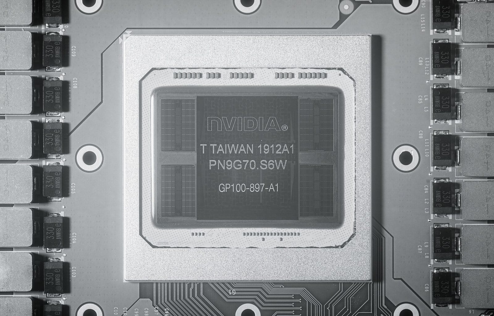
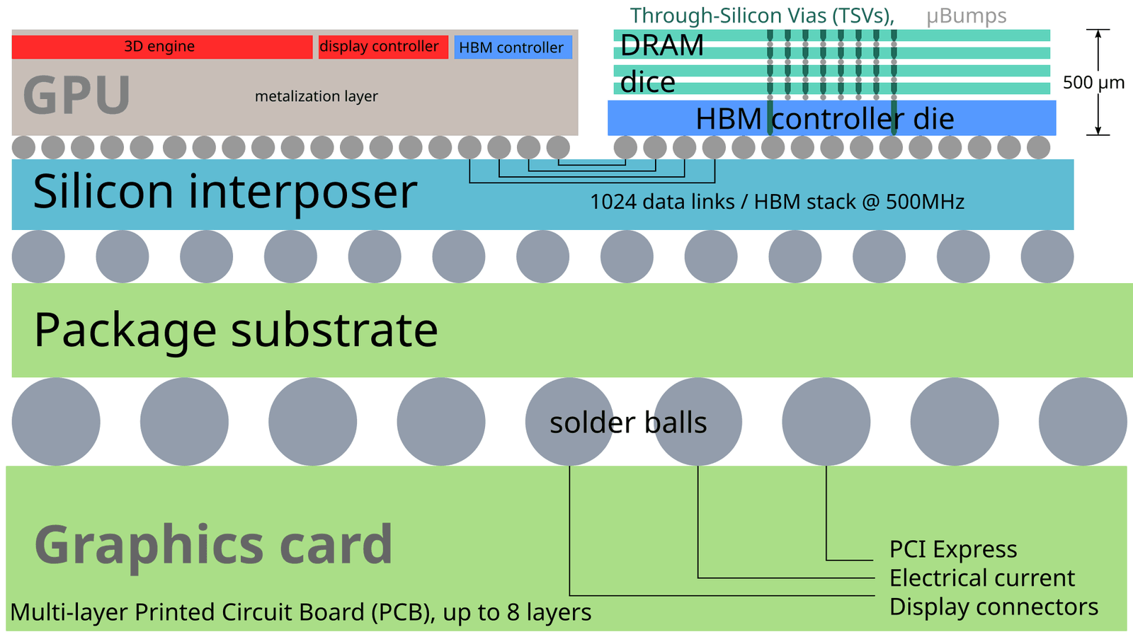
The switching has one more cost. The chip has to keep track of tens of thousands of threads, and giving each thread its own logic for fetching and decoding instructions would eat the area we wanted for arithmetic. How the threads are grouped, and where those groups live on the chip, is the next question.
03Threads, warps and streaming multiprocessors
3.1From the whole GPU down to one thread
Control logic is expensive, so threads don't each get their own. They run in groups of 32 called warps, and the 32 threads of a warp share one stream of instructions: the hardware issues one instruction and all 32 threads carry it out together, each on its own data. The chip is divided into streaming multiprocessors, or SMs. Each SM holds many warps at once and picks a ready one to issue from on every cycle.
An H100 SXM5 (the version that mounts on a server board) has 132 SMs, according to NVIDIA's Hopper architecture post. The full GH100 die has 144, and the PCIe card version has 114. Each SM is split into four partitions, and each partition has its own warp scheduler, the circuit that picks which warp issues next.
The unit a programmer chooses is the thread block (NVIDIA's hardware documents call it a CTA): a group of up to 1,024 threads that run on one SM, share its fast memory and can synchronise with each other. All the blocks of one launch together are called the grid. For the brighten job we pick 256 threads per block, a free choice, and the arithmetic falls out:
| Pixels, so threads | 3840 × 2160 | 8,294,400 |
| Threads per block | our choice | 256 |
| Blocks in the grid | 8,294,400 / 256 | 32,400 |
| Warps per block | 256 / 32 | 8 |
| Warps in the grid | 32,400 × 8 | 259,200 |
| blocks each of 132 SMs works through | ≈ 245 | |
What the hardware schedules is the warp: 32 consecutive threads of a block. NVIDIA's programming guide is blunt about it: "A warp executes one common instruction at a time, so full efficiency is realized when all 32 threads of a warp agree on their execution path."
That model is called SIMT, single instruction, multiple threads. Each thread has its own registers and, since NVIDIA's Volta generation, its own program counter (the marker of which instruction it's on), so you write ordinary scalar code for one thread. Underneath, 32 of those threads march in lockstep.
3.2How a scheduler hides a memory stall
Now we can watch the trick from section 2.2 happen. The CC 9.0 architecture notes (compute capability 9.0 is NVIDIA's label for Hopper's feature limits) say an SM "statically distributes its warps among its schedulers. Then, at every instruction issue time, each scheduler issues one instruction for one of its assigned warps that is ready to execute, if any."
Here is one scheduler with four warps from a brighten block. Each warp has to load its 32 pixels from HBM, add 0.1 and store them. To keep the picture small the scheduler has only four warps, far fewer than a real one.
brighten, each owning 32 pixels. All four are ready, and the issue slot is empty.An SM runs four of these schedulers side by side, each picking one ready warp per issue slot, and that is all the hardware does to hide memory latency: no prediction and no reordering, only enough waiting warps that one is always ready. NVIDIA publishes little about what happens below this level, such as how a scheduler chooses among several ready warps.
3.3The register file sets occupancy
An SM's register file is 256 KB, which is 65,536 32-bit registers, as big as its L1 cache and shared memory put together.
?Why is the register file so big?
Because every resident warp's registers live there for the warp's whole life. NVIDIA's programming guide says the execution context "is maintained on-chip during the entire lifetime of the warp. Therefore, switching from one execution context to another has no cost." The file has to be big enough to hold the registers of all the warps we want to switch between.
An SM can hold at most 64 warps, which is 2,048 threads, on compute capability 9.0. The fraction of those 64 slots that are filled is called occupancy, and registers are usually what caps it. A thread that needs many registers leaves room for fewer threads. A small kernel like brighten needs few registers, so its blocks fit easily, but here is a heavier kernel to show the arithmetic:
| Registers per SM | Hopper, CC 9.0 | 65,536 |
| Threads for full occupancy | 64 warps × 32 | 2,048 |
| Register budget per thread at 100% | 65,536 / 2,048 | 32 |
| A kernel that needs 128 registers | 65,536 / 128 | 512 threads |
| Warps resident | 512 / 32 | 16 of 64 |
| occupancy for a 128-register kernel | 25% | |
?Is 25% occupancy bad?
Not necessarily. Occupancy only exists to hide latency: you need enough ready warps that, on each cycle, a scheduler finds one whose operands have arrived. A kernel with lots of independent loads per thread can hide latency with few warps, and many of the fastest matrix-multiply kernels run at low occupancy on purpose, trading warps for registers. A kernel that issues one load and then waits on it, like brighten, needs every warp it can get.
3.4Five kinds of memory, very different sizes
Registers are one of several places a thread's data can live. Here are all five levels on an H100 SXM5, from the smallest and fastest to the largest:
| Level | H100 SXM5 size | Who sees it | What lives there |
|---|---|---|---|
| Registers | 256 KB per SM | One thread | Every live variable of every resident warp |
| Shared memory / L1 | 256 KB per SM, up to 228 KB as shared | One thread block | Tiles you load on purpose, so a kernel avoids going to HBM twice for the same bytes |
| L2 | 50 MB | Whole GPU | Whatever the hardware decides |
| HBM3 | 80 GB at 3.35 TB/s | Whole GPU | The data the kernels work on: our photo here, and a model's weights and caches in section 6 |
| Host DRAM | Whatever the server has | Reached over a link to the host (section 6.4) | Your dataset and staging buffers |
Sizes are from the Hopper post and the CC 9.0 section of the programming guide. Shared memory is the one level with no CPU equivalent: a scratchpad that a thread block reads and writes explicitly, at on-chip speed. It's how serious GPU kernels avoid going to HBM twice for the same bytes. "IO-aware" usually means an algorithm rearranged so that its working tile fits there, and FlashAttention, one of the cards at the end of the chapter, is the best-known example. Brighten never needs it, because it touches each pixel once.
3.5What a GPU promises
Before the table, three terms. Peak arithmetic is counted in FLOPs, floating-point operations, where one add or one multiply of decimal numbers is one FLOP, and a teraFLOPS is a trillion of them per second. The H100 reaches its headline figure with tensor cores, units that multiply small blocks of numbers and add them to a running total, working in BF16, a 16-bit number format common in machine learning. Section 6 comes back to why tensor cores matter so much.
If you give a GPU enough independent work, here's the contract:
| It promises | It doesn't promise |
|---|---|
| Enormous aggregate arithmetic. An H100 SXM does 989 dense BF16 teraFLOPS on its tensor cores (NVIDIA's H100 page lists 1,979 with 2:4 sparsity, a pruning pattern that lets the hardware skip half the numbers; dense is half). | Any order between thread blocks, or that two blocks run at the same time |
| Enormous memory bandwidth. 3.35 TB/s from 80 GB of HBM3, on the same datasheet. | Anything about how fast a single thread goes. A lone GPU thread is slow. |
| Free switches between thread groups, since their state stays on-chip. | That the host keeps up. It runs whatever is in its queue and idles otherwise, and the queue is your problem. |
The contract has a condition buried in it: the 32 threads of a warp share one instruction stream, and their memory requests arrive together. Two things at warp granularity decide whether the machine is busy or only looks busy. One is what a warp does when its threads disagree at a branch, and the other is what it does when its 32 threads load from scattered addresses.
04What a warp does at a branch and at a load
4.1Divergence: both sides of the if
Change the brighten job slightly: brighten only the dark pixels, and leave the bright ones alone. The kernel now contains an if.
kernel brighten_dark(i):
    if in[i] < 0.5:  out[i] = in[i] + 0.1
    else:            out[i] = in[i]
Suppose the photo has a large shadow. Inside the shadow every pixel is dark, so a warp of 32 neighbouring pixels all take the first side, and the warp issues that one instruction for everyone. Suppose instead the photo is noisy, with dark and bright pixels mixed at random. Now nearly every warp contains threads that want the first side and threads that want the second, and one shared instruction stream can't do both at once.
What the hardware does is run both sides, one after the other. First the threads that took the if execute while the rest are switched off, then the others execute while the first group is switched off. This is called divergence. The warp's time is the sum of both sides, and each side runs with only part of the warp doing useful work.
A million threads each run 2,048 dependent FMAs (fused multiply-adds, one multiply and one add in a single instruction) on one of two paths, and half take each side. In run A the split falls between 32-wide groups; in run B it falls inside every group. How much longer is run B?
This kernel is written in Metal Shading Language, Apple's GPU language, which a small Swift program compiles and launches. Apple's name for a warp is a SIMD-group, and Metal reports its width, threadExecutionWidth, as 32 on Apple's GPUs. A threadgroup is Apple's thread block. In mode 0, all 32 threads of a SIMD-group take the same side. In mode 1, odd and even threads split inside every SIMD-group. Both modes send half the threads down each path.
kernel void diverge(device float* out    [[buffer(0)]],
                    constant uint& mode  [[buffer(1)]],
                    uint gid [[thread_position_in_grid]]) {
    // mode 0: all 32 threads of a SIMD-group take the same side
    // mode 1: odd and even threads split inside every SIMD-group
    bool odd = mode == 0 ? ((gid >> 5) & 1) : (gid & 1);
    float x = float(gid) * 1e-7f;
    if (odd) { for (int i = 0; i < 2048; i++) x = fma(x, 0.999f, 0.001f); }
    else     { for (int i = 0; i < 2048; i++) x = fma(x, 1.001f, -0.001f); }
    out[gid] = x;
}
// 1,048,576 threads, 256 per threadgroup, GPU timestamps, best of 7branch uniform per SIMD-group: 6.10 ms
branch splits every SIMD-group: 12.50 ms (2.05x)Half the threads take each side in both runs. All that changes is whether the split falls between SIMD-groups or inside them. Inside, each group executes both loops, and the kernel takes almost exactly twice as long. A second run gives nearly the same pair, 6.09 and 12.51 ms. A split into more than two paths would cost proportionally more, up to 32 times in the worst case, one pass per distinct path.
So a branch is cheap when neighbouring threads agree and expensive when they don't. The same neighbouring-thread idea decides what happens at a load.
4.2Coalescing: 32 addresses, how many transactions
Back to plain brighten. Our image is stored row by row: pixel (x, y) sits at byte offset (y × 3840 + x) × 4. If we give the 32 threads of a warp 32 pixels along one row, thread 0 reads bytes 0–3, thread 1 reads bytes 4–7, and the whole warp's request covers one unbroken 128-byte stretch. If instead we give the warp 32 pixels down one column, neighbouring threads read addresses 3840 × 4 = 15,360 bytes apart.
Memory doesn't hand out single bytes. When the 32 threads of a warp issue a load, the hardware merges their addresses into as few memory transactions as it can, and a transaction moves a whole 32-byte sector. NVIDIA's Best Practices Guide states the rule for compute capability 6.0 and later: accesses "coalesce into a number of transactions equal to the number of 32-byte transactions necessary to service all of the threads of the warp." This merging is called coalescing.
The same count in a table:
| Warp access pattern | 32-byte sectors fetched | Useful bytes per sector |
|---|---|---|
| 32 threads read 32 adjacent floats | 4 | All 32 |
| 32 threads read floats 128 bytes apart | 32 | 4 of 32; the other 28 are thrown away |
We can measure this. This next kernel makes every thread read exactly one float from a 256 MiB buffer of 64 million floats. The line idx = (gid % rows) * stride + gid / rows is a permutation, so whatever the stride, every float is read exactly once. What changes is how far apart the addresses of neighbouring threads are. The test v == 12345.0f is never true, but it stops the compiler from deleting the load. A Swift host program, not shown, launches 64 million threads in groups of 256 and times each run with the GPU's own timestamps, keeping the best of 7.
kernel void gather(device const float* a [[buffer(0)]],
                   device float* out     [[buffer(1)]],
                   constant uint& n      [[buffer(2)]],
                   constant uint& stride [[buffer(3)]],
                   uint gid [[thread_position_in_grid]]) {
    uint rows = n / stride;
    uint idx = (gid % rows) * stride + gid / rows;   // a permutation of 0..n-1
    float v = a[idx];
    if (v == 12345.0f) out[0] = v;                   // never true; keeps the load
}
// n = 64M floats (256 MiB), 64M threads, 256 per threadgroupstride 1 floats ( 4 B apart): 2.40 ms useful 111.9 GB/s
stride 2 floats ( 8 B apart): 4.81 ms useful 55.8 GB/s
stride 4 floats ( 16 B apart): 9.82 ms useful 27.3 GB/s
stride 8 floats ( 32 B apart): 20.12 ms useful 13.3 GB/s
stride 16 floats ( 64 B apart): 42.25 ms useful 6.4 GB/s
stride 32 floats ( 128 B apart): 43.99 ms useful 6.1 GB/s
stride 64 floats ( 256 B apart): 45.38 ms useful 5.9 GB/sEvery row reads each of the 64 million floats exactly once, and a second run agrees to within 6% on every row. Time doubles with every doubling of the stride up to 64 bytes, then stops. The picture is easier to see as a curve:
Stride 1 reaches 112 GB/s, 93% of the 120 GB/s of memory bandwidth that Apple quotes for its M4 laptop and desktop chip. Each doubling after that halves the useful bandwidth, which is what you'd expect if every thread drags in a whole transaction to use 4 bytes of it. The curve flattens at 64 bytes, and why is still open. If the hardware fetched in 32-byte units, as NVIDIA's does, the curve would go flat at 32 bytes. If it fetched whole 128-byte cache lines (the CPU's line size on Apple silicon, from chapter 02), it would keep falling until 128. A memory path that moves 64 bytes at a time would fit the curve, but Apple doesn't document it and the numbers alone can't prove it. Xcode's GPU counters for bytes read from DRAM would settle it.
Now section 1.2's result makes sense. A plain C++ sum over the same 256 MiB on the CPU (clang++ -O2, eight accumulators per thread) reached 55 GB/s on one thread and 106 to 108 GB/s on ten. The GPU's 112 GB/s is barely ahead, because the CPU and the GPU draw on one pool of DRAM, so neither has more bandwidth to offer. An H100's advantage lives in the HBM stacks beside the die, and a laptop doesn't have any.
That covers what a kernel does once it's running on an SM. But our 8.3 million threads begin as a single line of code on the host, and section 1.4 found a fixed cost every time work crosses over. What happens in that hand-off?
05What happens when you launch a kernel
5.1From your thread to a warp
On an NVIDIA GPU, with CUDA (NVIDIA's programming platform for its GPUs), the brighten launch is one line of host code: brighten<<<32400, 256>>>(in, out). The numbers in the triple angle brackets are the grid size and the block size from section 3.1. Between that line and the first warp issuing an instruction, a lot happens, and much of it lives in NVIDIA's closed userspace driver. But the hardware interface is documented, and an open-source driver shows the software side. That driver is Mesa's NVK, which drives the same NVIDIA GPUs through Vulkan, a cross-vendor interface for graphics and compute. Here is the whole path first, with each piece named as it appears. The subsections after it read the real documents and source files behind each step.
brighten<<<32400, 256>>>. Everything so far is ordinary user-space code. The driver first writes a launch descriptor into memory, which NVIDIA calls a QMD: grid size, block size, register count, shared memory and the program's address.At the end, each SM's four warp schedulers issue one instruction per slot from a ready warp, exactly as in section 3.2, and the kernel is running.
5.2No syscall on the launch path
?Isn't a kernel launch a system call?
It's natural to expect one. Chapter 07 spent a whole section on what a system call costs, and a GPU driver paying one per launch would seem obvious. It doesn't. Work reaches the GPU through memory the process has already mapped, and NVIDIA's own reference manual lists the steps:
NOTIFY_CHANNEL_PENDING - Notify Host that a channel has new work available

     NOTIFY_CHANNEL_PENDING is known as the channel doorbell register.  Writing
a channel's opaque handle to the NOTIFY_CHANNEL_PENDING register (sometimes
referred to as "ringing the doorbell") tells Host that new work is available to
run on that channel.
...
     Submitting new work to a channel involves the following steps:

     1. Write methods to a pushbuffer segment
     2. Construct a new GP entry pointing to that pushbuffer segment
     3. Update GP_PUT in USERD to indicate the new GP entry is ready
     4. Request the doorbell handle from RM, given the channel ID
     5. Write the channel's handle to the NOTIFY_CHANNEL_PENDING register
Two words in it need translating. Host, with a capital H, is NVIDIA's name for the unit at the GPU's front end that fetches commands, the "GPU front end" in the scene; it has nothing to do with the host CPU program from section 1.1. A channel is one queue of work into the GPU, with its own pushbuffer and GPFIFO, and a process sets up its channels once, when it starts using the GPU. USERD is a small block of memory per channel that holds indices such as GP_PUT.
Step 4 happens once, at channel setup. RM, NVIDIA's resource manager, is the part of the driver that runs inside the operating-system kernel, so that step is a system call. Steps 1, 2, 3 and 5 are ordinary stores from your process, repeated for every launch. Here are the pieces the list names, as they appeared in the scene:
| Piece | What it is |
|---|---|
| Pushbuffer | A ring of commands ("methods") in memory |
| GPFIFO | A ring of 8-byte entries pointing into the pushbuffer |
GP_PUT | The producer index into the GPFIFO |
| Doorbell | The NOTIFY_CHANNEL_PENDING register that tells Host to look |
If that sounds like io_uring's submission queue from chapter 07, it's the same idea, older: a queue in shared memory that one side fills and the other drains, so the common case needs no trip into the operating-system kernel.
This document is for Turing (TU104), an earlier generation, and it warns that the handle format "is subject to change in future chips". This chapter assumes Hopper keeps the same shape, though no Hopper manual found so far confirms it.
5.3What the driver writes into the pushbuffer
NVIDIA gives each generation's command interface a class name, such as TURING_COMPUTE_A or HOPPER_COMPUTE_A, and the class defines which methods a driver may send. CUDA's userspace driver is closed, so to see the method stream we read NVK, which drives the same compute classes. Its vkCmdDispatch path (Vulkan's name for a kernel launch) uploads a QMD, then pushes two methods: "here's the QMD's address" and "schedule it".
   uint64_t qmd_addr = 0;
   VkResult result = nvk_cmd_flush_cs_qmd(cmd, &cmd->state, global_size,
                                          &qmd_addr, NULL);
   ...
   struct nv_push *p = nvk_cmd_buffer_push(cmd, 7);
   ...
   P_MTHD(p, NVA0C0, SEND_PCAS_A);
   P_NVA0C0_SEND_PCAS_A(p, qmd_addr >> 8);

   if (nvk_cmd_buffer_compute_cls(cmd) <= TURING_COMPUTE_A) {
      P_IMMD(p, NVA0C0, SEND_SIGNALING_PCAS_B, {
            .invalidate = INVALIDATE_TRUE,
            .schedule = SCHEDULE_TRUE
      });
   } else {
      P_IMMD(p, NVC6C0, SEND_SIGNALING_PCAS2_B,
             PCAS_ACTION_INVALIDATE_COPY_SCHEDULE);
   }
NVK reserves seven 32-bit words of pushbuffer for this. The QMD itself sits elsewhere in GPU memory, with its address shifted right by 8, so presumably 256-byte aligned.
NVK picks the QMD version by compute class: Hopper (HOPPER_COMPUTE_A) gets version 4, the layout quoted in section 5.4, per nak/qmd.rs. Whether CUDA writes exactly these methods isn't public. It targets the same class, so it can't be far off.
5.4What a launch looks like as bytes
NVIDIA publishes the QMD layout for Hopper's compute class in its open documentation repo. These are real field offsets, in bits:
#define NVCBC0_QMDV04_00_SHARED_MEMORY_SIZE             MW(601:584)
#define NVCBC0_QMDV04_00_GRID_WIDTH                     MW(1055:1024)
#define NVCBC0_QMDV04_00_GRID_HEIGHT                    MW(1071:1056)
#define NVCBC0_QMDV04_00_GRID_DEPTH                     MW(1103:1088)
#define NVCBC0_QMDV04_00_CTA_THREAD_DIMENSION0          MW(1167:1152)
#define NVCBC0_QMDV04_00_CTA_THREAD_DIMENSION1          MW(1183:1168)
#define NVCBC0_QMDV04_00_CTA_THREAD_DIMENSION2          MW(1199:1184)
#define NVCBC0_QMDV04_00_REGISTER_COUNT                 MW(1208:1200)
#define NVCBC0_QMDV04_00_BARRIER_COUNT                  MW(1215:1211)
#define NVCBC0_QMDV04_00_PROGRAM_ADDRESS_LOWER          MW(1247:1216)
#define NVCBC0_QMDV04_00_PROGRAM_ADDRESS_UPPER          MW(1272:1248)
#define NVCBC0_QMDV04_00_OCCUPANCY_MAX_WARP             MW(1295:1288)
#define NVCBC0_QMDV04_00_OCCUPANCY_MAX_REGISTER         MW(1311:1304)
#define NVCBC0_QMDV04_00_CONSTANT_BUFFER_ADDR_LOWER_SHIFTED6(i) \
                                          MW((1567+(i)*64):(1536+(i)*64))
For brighten, GRID_WIDTH would hold 32,400 and CTA_THREAD_DIMENSION0 would hold 256. Read the list as a checklist for placing blocks: how many, how big, and REGISTER_COUNT plus SHARED_MEMORY_SIZE, the two numbers that decide how many blocks fit on one SM at once. That is section 3.3's occupancy arithmetic, done in silicon. Kernel arguments, such as the addresses of in and out, go in a constant buffer whose address is also in the descriptor.
5.5From the queue to an SM
After the doorbell, the public detail thins out quickly. The PBDMA, the part of Host that reads command memory, reads GP_PUT, fetches the pushbuffer segment, and forwards compute methods to the compute front end, which reads the QMD. NVIDIA's whitepapers have described the next piece since the Fermi generation: "The GigaThread global scheduler distributes thread blocks to SM thread schedulers" (Fermi whitepaper).
?Why does a big grid run in waves?
A block goes onto an SM only if that SM has room for all of it at once: free registers, shared memory and warp slots. Blocks that don't fit wait for earlier ones to retire. For brighten, suppose each thread needs 32 registers or fewer, a plausible figure for a kernel this small. Then an SM's 2,048 thread slots hold 8 blocks of 256 at a time:
| Blocks resident per SM | 2,048 threads / 256 | 8 |
| Blocks resident on the GPU | 132 SMs × 8 | 1,056 |
| Blocks in the grid | from section 3.1 | 32,400 |
| the grid runs as about this many waves across the SMs | ≈ 31 | |
A wave is a loose picture, since a new block is placed as soon as an old one finishes, but it gives the right sense of scale: the 8.3 million threads never exist at once, and the hardware feeds them through in batches of roughly 270,000 (1,056 blocks of 256).
5.6What a launch costs
Every launch pays for the path above, which costs microseconds of CPU and queue time. In NVIDIA's CUDA Graphs post, a V100 kernel that executed in 2.9 µs cost 9.6 µs per kernel with a sync after each, 3.8 µs launched back to back on a stream (an in-order queue of GPU work), and 3.4 µs when the whole sequence was captured into a CUDA graph, a recorded list of launches that the driver can replay with one submission.
The laptop GPU from the earlier experiments shows the same shape. Metal submits work in command buffers, its version of a batch of pushbuffer methods, and the host commits a command buffer and can then wait for it to finish. Here an empty 32-thread kernel is launched 2,000 times, first committing and waiting for each one separately, then encoding all 2,000 into a single command buffer:
Metal's round trip is much slower than CUDA's, and most of those 100 µs are probably the CPU thread waking up on completion, not the GPU. The shape is the same on both vendors, though: submission is cheap only when it's batched.
Put that against the brighten job. Brightening one 4K photo on an H100 means moving 66 MB. At the datasheet's 3.35 TB/s that's about 20 µs, as a best case. A launch like the V100's 3.8 to 9.6 µs is then a large fraction of the whole job, and a program that brightens many photos with one launch each, waiting after every one, would spend roughly a sixth to a third of its time on launches. That's the fixed cost from section 1.4 in its data-centre form. Once the kernel is running, though, what sets its speed? Brighten's 20 µs came from moving bytes, and the arithmetic hardly mattered. The next section turns that observation into a rule.
06Bytes per FLOP: what limits a kernel
6.1Two ceilings and a ridge point
Every kernel does some number of FLOPs and moves some number of bytes to and from HBM. Brighten does 1 FLOP per pixel and moves 8 bytes (4 in, 4 out), so 1/8 FLOP per byte. The ratio is called arithmetic intensity, in FLOPs per byte. A roofline model (Williams, Waterman and Patterson, CACM 2009) says a kernel's attainable throughput is the lower of two ceilings: the chip's peak compute, or its memory bandwidth times the kernel's intensity.
| Peak dense BF16 tensor compute | H100 SXM, datasheet 1,979 sparse ÷ 2 | 989 TFLOP/s |
| Peak HBM3 bandwidth | H100 SXM datasheet | 3.35 TB/s |
| Ridge point | 989 × 10¹² / 3.35 × 10¹² | ≈ 295 FLOP/byte |
| a kernel below ~295 FLOP/byte is waiting on memory, not math | 295 | |
The ridge point is the intensity where the two ceilings meet. Below it a kernel is memory-bound: it waits on HBM, and more tensor cores wouldn't help at all. Above it, the kernel is compute-bound. An H100's ridge is very high, and it has been climbing for generations because FLOPs have grown faster than bandwidth.
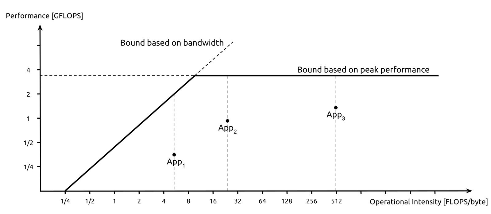
Tensor cores are why the ceiling is so high. Plain FP32 (32-bit floats, like our photo) on the SM's ordinary arithmetic units, which NVIDIA calls CUDA cores, is 67 TFLOPS on the same datasheet, roughly a fifteenth of the dense BF16 tensor rate. Tensor cores only do matrix multiply-accumulate. In a machine-learning model, every step that isn't a matrix multiply (the many small per-element steps between the multiplies, much like brighten) runs on the CUDA cores, and usually at low intensity too.
Brighten runs on the CUDA cores, in FP32. Its own ridge is 67 / 3.35, about 20 FLOP/byte, and at 1/8 FLOP per byte it sits about 160 times below it. An elementwise add in BF16 (one FLOP per 6 bytes: two operands in, one result out) is about 1,800 times below the 295 ridge. Adds don't run on tensor cores either, so the ridge that applies is lower, and the conclusion stays the same. A matrix multiply of two big square matrices is the opposite case. If each number moved only once, an n×n FP32 multiply would do 2n³ FLOPs on 12n² bytes, an intensity of n/6, roughly 680 FLOP/byte at n = 4096. That's why the matrix multiply in section 1.3 pulled ahead of the CPU as it grew and brighten didn't.
6.2Decoding one token of a 70B model
Brighten is a small version of a workload that fills data centres: running a large language model. A language model produces text one token (a short piece of a word) at a time. To produce each token, it runs its input through every layer of the network, and the network's learned numbers, its weights, have to be read to do it. This one-token-after-another phase of generation is called decode.
Take Meta's Llama 3 70B, a model with 80 layers and about 70 billion weights (Table 3 of the Llama 3 paper). In BF16, 2 bytes each, that's 140 GB, which doesn't fit on one 80 GB H100, so the usual deployment splits it over two with tensor parallelism, meaning each layer's weights are divided between the two GPUs.
At batch 1 (one request being decoded), every one of those weights is used for exactly one multiply and one add per token. That makes decode brighten's big cousin: read an enormous amount of data once and do almost no arithmetic on it. Each request also keeps a KV cache, the keys and values the model already computed for the earlier tokens of its text so that it doesn't recompute them, and section 6.3 sizes it. Here is one decode step at batch 1, then at batch 32:
Here is the batch-1 arithmetic in full:
| Weight bytes read per token | 70 × 10⁹ params × 2 B | 140 GB |
| FLOPs per token | 2 × 70 × 10⁹ | 140 GFLOP |
| Arithmetic intensity | 140 GFLOP / 140 GB | 1 FLOP/byte |
| Time to read the weights | 140 GB / (2 × 3.35 TB/s) | 20.9 ms |
| Time to do the math | 140 GFLOP / (2 × 989 TFLOP/s) | 0.07 ms |
| Ceiling on tokens per second | 1 / 20.9 ms | ≈ 48 |
| fraction of tensor-core peak used at batch 1 | ≈ 0.34% | |
One FLOP per byte against a ridge of 295. That's what people mean by decode is memory-bandwidth-bound, and it follows from the arithmetic, whatever framework runs it. These are ceilings. Real servers reach some fraction of peak bandwidth, and on top of that the two GPUs have to swap partial results after each layer, over a link called NVLink (section 6.4).
?Why does FP8 let one GPU do the job of two?
FP8 is an 8-bit number format, so each weight takes one byte. Quantising, which means storing weights in fewer bits, down to FP8 makes the 70 GB of weights fit on one GPU. One H100 reading 70 GB takes the same 20.9 ms as two reading 140 GB. Half the hardware gives the same per-token latency ceiling, because the only thing that mattered was bytes per unit of bandwidth.
6.3Batching and the KV cache
Run 32 sequences together and the weights are read once for all of them, so intensity on the weight matrix multiplies rises to about 32 FLOP/byte. That's why continuous batching, serving many requests in one step and swapping finished sequences for new ones, is the first thing every inference server does.
But each sequence carries its own KV cache, and it sits in HBM next to the weights. To produce a new token, a step in every layer called attention looks back at every earlier token in that sequence, and it does so through stored vectors: a key and a value for each earlier token. Attention is split into parallel copies called heads, and Llama 3 70B has 64 query heads, each working on vectors of 128 numbers. Its keys and values are shared in groups, so each layer stores only 8 key/value heads per token. That gives the cache's size, and attention reads all of it on every step:
| KV bytes per token | 2 (K,V) × 80 layers × 8 heads × 128 dim × 2 B | 320 KiB |
| 32 sequences × 2,000 tokens of context | 64,000 × 327,680 B | 21 GB |
| Attention intensity per cached token | 64 query heads × 512 FLOP / 4,096 B per layer | 8 FLOP/byte |
| Bytes per step | 140 GB weights + 21 GB KV | 161 GB |
| Step time, 2 × H100 | 161 GB / 6.7 TB/s | 24 ms |
| aggregate ceiling at batch 32 vs 48 tok/s at batch 1 | ≈ 1,330 tok/s | |
That is 28 times the throughput of batch 1 for 15% more time per step.
?Why doesn't batching fix attention too?
Look at the attention row: 8 FLOP/byte however big the batch gets, because no two sequences share a cache. The 8 comes from the grouping above, which is called grouped-query attention: 64 query heads reuse the same 8 key/value heads, so each cached byte feeds eight heads' worth of arithmetic. With one key/value head per query head it would be 1.
Then there's capacity. Two H100s have 160 GB, the weights take 140, and what's left is about 20 GB before the model's intermediate results and the driver's own per-process state take their share. At 320 KiB per token that's at most about 61,000 tokens of KV in flight across all requests. Servers that reserve room for each request's maximum length up front waste 60 to 80% of it (section 7.3 has the source), and then you're down to 12,000 to 24,000, and the batch size you can run (the throughput you're paying for) drops with it.
6.4Getting data to the GPU
Section 5.6 said launches are cheap only when batched, and decode shows why that matters. Eighty layers at several kernels each is hundreds of launches per token in eager mode, where each operation is launched as the program reaches it. At a few microseconds each, that's milliseconds against the 20.9 ms memory floor. So vLLM, a widely used open-source LLM serving system, captures decode steps as CUDA graphs unless you pass enforce_eager.
Weights and requests also have to reach the GPU in the first place, over links that are much slower than HBM. PCIe is the general-purpose bus between host and GPU, and NVLink is NVIDIA's faster link between GPUs. NVIDIA's datasheet gives each link as a total of both directions:
| Link | Datasheet figure | One direction | Relative to HBM |
|---|---|---|---|
| HBM3, on package | 3.35 TB/s | n/a | 1× |
| NVLink 4, GPU to GPU | 900 GB/s total | 450 GB/s | ≈ 1/7 |
| PCIe Gen5 x16, to host | 128 GB/s total | 64 GB/s | ≈ 1/52 |
The last column compares one direction against HBM. (On some systems the host link is NVLink-C2C, NVIDIA's link between a host CPU and a GPU, instead of PCIe.) Loading one GPU's 70 GB half of the model from host memory takes about 1.1 s at PCIe line rate, and in practice longer. Moving one 2,000-token request's KV cache (655 MB) over NVLink takes roughly 1.5 ms. Anything crossing PCIe inside the per-token loop is a mistake.
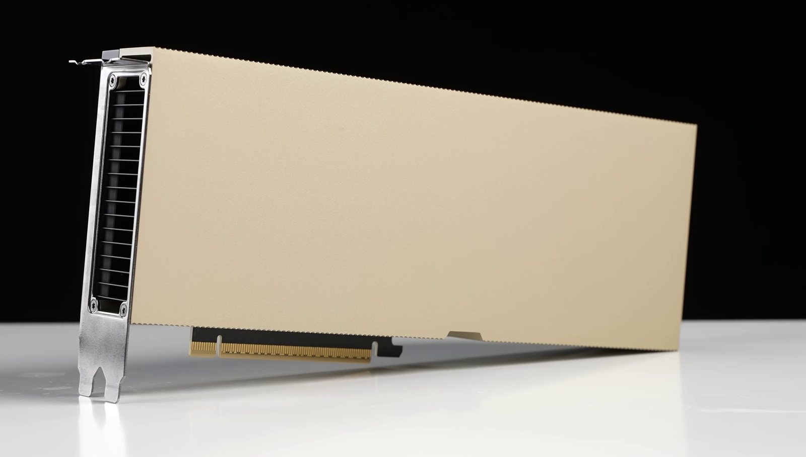
Two features of the CUDA runtime address the host side. Ordinary memory is pageable: the operating system may move or swap out its pages (chapter 04), so a device can't safely copy from it directly. Copying from it means the driver first copies into a temporary page-locked buffer, memory the operating system promises to leave in place, and starts a DMA from there (direct memory access, where the device copies the data itself without the CPU), per NVIDIA's data transfer post. Allocating pinned memory (cudaMallocHost, or pin_memory=True in a PyTorch DataLoader) skips that copy and lets cudaMemcpyAsync overlap with compute on a stream. Unified memory (cudaMallocManaged) gives CPU and GPU one pointer and migrates pages on fault, and cudaMemPrefetchAsync moves pages ahead of time.
Everything so far assumes the hardware works. Brighten lasts 20 µs, but a training run uses the same chips for weeks, and over weeks the chips break.
07How GPUs fail
7.1Four hundred and nineteen interruptions in 54 days
Probably the best public data on GPU failure at scale is in Meta's Llama 3 paper, section 3.3.4. Training the 405B model on up to 16K H100s, they logged 466 job interruptions in a 54-day window: 47 planned and 419 unexpected. "Approximately 78% of the unexpected interruptions are attributed to confirmed hardware issues ... or suspected hardware-related issues like silent data corruption."
| Root cause (Table 5) | Count | Share of unexpected |
|---|---|---|
| Faulty GPU | 148 | 30.1% |
| GPU HBM3 memory | 72 | 17.2% |
| Software bug | 54 | 12.9% |
| Network switch / cable | 35 | 8.4% |
| Host maintenance, unplanned | 32 | 7.6% |
| GPU SRAM memory | 19 | 4.5% |
| GPU system processor | 17 | 4.1% |
| Silent data corruption | 6 | 1.4% |
| GPU thermal interface and sensor | 6 | 1.4% |
This table lists the largest causes, with the counts and percentages as the paper prints them. Meta's paper classes six of these rows as GPU issues: faulty GPU, HBM3, SRAM, system processor, silent data corruption and the thermal interface and sensor. Those six add up to 58.7% of all unexpected interruptions, the paper's own figure. One oddity: 148 of 419 would be 35.3%, not 30.1%, while every other row matches its count, so we keep the paper's printed figures as they stand. HBM alone caused more interruptions than every network problem in the table combined.
?Why does one bad GPU matter so much?
A training job spreads one model over many GPUs, each driven by its own process called a rank, and the ranks exchange results with collective operations through NVIDIA's NCCL library. A job that's synchronous across every GPU stops when one chip does, so one bad chip stops all 16,000. That's why the paper's headline reliability number is effective training time (above 90%) and not uptime. At 419 unexpected interruptions in 54 days, a job like this stops roughly eight times a day, and automation handled all but three of the interruptions without a person getting involved.
Two more details from that section. Failures over NVLink "often manifest as stalled load/store operations within CUDA kernels without returning a clear error code", so a dead link looks like a hang and not like an error. And the team saw a 1 to 2% diurnal throughput swing, with mid-day temperatures pushing GPUs to lower clocks.
7.2Xid: the error the driver writes to your kernel log
When the NVIDIA driver sees a GPU error it prints an Xid to the operating system's kernel log (what dmesg shows), a numbered code you can search for with NVRM: Xid. From NVIDIA's Xid documentation (release 615): Xids indicate "the driver programming the GPU incorrectly or ... corruption of the commands sent to the GPU". They can mean a hardware problem, a driver bug, or your application. Several of the entries below mention ECC, error-correcting code, the extra bits stored with memory that let it repair a single flipped bit and detect two. These are the ones a fleet should expect to see most:
| Xid | Meaning | Catalog action |
|---|---|---|
| 13, 31 | Graphics engine exception; GPU memory page fault. Usually your code: an out-of-bounds access in a kernel. | Restart the application |
| 48 | Double-bit ECC error: HBM returned data ECC couldn't correct | Reset the GPU, or drain and reset if 63 or 64 comes with it |
| 63 | Memory row remapping event: the GPU retiring a bad HBM row | Listed as ignorable |
| 64 | Row remapping failure: it couldn't retire the row | Reset the GPU and contact support |
| 79 | "GPU has fallen off the bus": the host can't reach it over PCIe | Restart the machine |
| 94 | Contained memory error | Restart the application that consumed the bad memory |
| 95 | Uncontained memory error | Not contained; the GPU needs a reset |
Your fleet's real policy is a mapping from each Xid to keep serving, restart the job, or drain and repair. The catalog is a starting point for it.
7.3Failures that log nothing
Plenty of GPU failures are the software kind, and they never produce an Xid:
- KV cache out-of-memory (OOM) and fragmentation. An inference server that reserves a max-length KV buffer per request runs out of HBM long before it runs out of compute. vLLM's authors measured existing systems wasting 60 to 80% of KV memory, partly to over-reservation and partly to fragmentation, free space broken into gaps too small to use (vLLM blog).
- Dataloader starvation. The dataloader is the code that reads and prepares each training batch. When it's slow, the GPU waits for the CPU to decode the next batch, and no GPU metric tells you why.
- Stragglers. A GPU that works but runs slow holds every rank back. From the Llama 3 paper: "Even a single straggler can slow down thousands of other GPUs."
- Silent data corruption. Six of Meta's 419 interruptions. Scarier is the kind that doesn't interrupt anything and just produces a wrong gradient, one of the numbers training uses to adjust the model.
Most of these leave the number everyone watches looking healthy, and that number deserves a closer look.
08Measuring a GPU in production
8.1What 100% in nvidia-smi measures
This is probably the most misread number in GPU operations. NVIDIA's nvidia-smi manual defines GPU utilization as "Percent of time over the past sample period during which one or more kernels was executing on the GPU. The sample period may be between 1 second and 1/6 second depending on the product."
Notice the words "one or more kernels". The definition says nothing about how many SMs, how many warps, or whether the tensor cores did anything. Work it through for a variation of brighten that launches a single block of 32 threads and spins:
| Metric | Reading |
|---|---|
| nvidia-smi utilization | 100%, because a kernel is always running |
| SMs with any work | 1 of 132, about 0.8% |
| Warp slots filled on that one SM | 1 of 64 |
Batch-1 decode from section 6.2 would show close to 100% too, with the tensor cores at a third of a percent.
?So what should you look at?
DCGM (NVIDIA's Data Center GPU Manager) has profiling metrics that mean something:
| DCGM field | Definition (NVIDIA's words) | Tells you |
|---|---|---|
| PROF_SM_ACTIVE (1002) | fraction of time at least one warp was active on a multiprocessor, averaged over all multiprocessors | Whether the SMs have work at all |
| PROF_SM_OCCUPANCY (1003) | fraction of resident warps on a multiprocessor, relative to the maximum | Whether latency can be hidden |
| PROF_PIPE_TENSOR_ACTIVE (1004) | fraction of cycles the tensor (HMMA / IMMA) pipe was active | Whether you're using what you paid for |
| PROF_DRAM_ACTIVE (1005) | fraction of cycles where data was sent to or received from device memory | Whether you're memory-bound |
(HMMA and IMMA are the tensor cores' matrix instructions for floating-point and integer data.) For LLM decode, DRAM active high and tensor active low is the expected, healthy shape. For training, tensor active low usually means something upstream is starving the GPU.
8.2The commands
Each question this chapter raised has a tool that answers it on a running machine.
# Is the GPU doing useful work, or only running a kernel? (sections 3 and 8.1)
nvidia-smi
nvidia-smi --query-gpu=utilization.gpu,memory.used,temperature.gpu,clocks.sm --format=csv -l 1
dcgmi dmon -e 1002,1003,1004,1005      # SM active, occupancy, tensor, DRAM

# Is the hardware healthy? (section 7.2)
dmesg -T | grep 'NVRM: Xid'
nvidia-smi -q -d ECC,ROW_REMAPPER

# Are the links up, and at what width? (section 6.4)
nvidia-smi nvlink --status
nvidia-smi topo -m
lspci -vv -s <bus-id> | grep -E 'LnkSta|LnkCap'

# Where did the time go? (sections 4, 5.6 and 6) Timeline first, then one kernel in depth
# nsys is Nsight Systems (a timeline of kernels and copies); ncu is Nsight Compute (one kernel's counters)
nsys profile --trace=cuda,nvtx,osrt ./app
ncu --section SpeedOfLight --section Occupancy -k <kernel> ./app
A PCIe link that trained at x8 instead of x16, or at Gen4 instead of Gen5, is a classic silent halving, and lspci's LnkSta shows it.
8.3Rules that hold up
- Read DCGM before nvidia-smi. SM active, tensor active and DRAM active say what the chip is doing, and utilization only says a kernel was running.
- Count bytes before FLOPs. Work out a kernel's arithmetic intensity first. Below the ridge, only fewer bytes help.
- Batch your launches. Hundreds of tiny kernels per step belong in CUDA graphs or fused kernels.
- Keep PCIe out of the hot loop. Stage data with pinned memory and prefetch, and leave weights and KV cache in HBM.
- Treat a fleet's hardware errors as routine. Map each Xid to an action ahead of time, and expect a synchronous job to stop whenever any one GPU does.
8.4What you give up
| You get | You pay | When the bill arrives |
|---|---|---|
| 989 dense BF16 TFLOPS | Only for matmuls, and only above ~295 FLOP/byte | On every decode step, which runs at 1 |
| 3.35 TB/s of HBM | 80 GB of it, shared by weights and every request's KV cache | When the batch you want doesn't fit |
| Free switching between warps | Registers per thread cap how many warps fit | As a kernel that spills or runs at 25% occupancy |
| SIMT: write scalar code | 32 threads share one instruction stream | When a branch splits a warp and runs both sides |
| A launch path with no syscall | Microseconds per launch anyway | In a decode loop with hundreds of kernels per token |
| A synchronous job across 16K GPUs | One bad GPU stops all of them | About eight times a day, going by Llama 3's numbers |
8.5Symptom, cause, fix
| Symptom | Likely cause | Fix |
|---|---|---|
| nvidia-smi at 100%, throughput low | Kernels running, but few SMs or tensor cores busy | Check DCGM 1002–1005 before anything else |
Gaps between kernels in an nsys timeline | Dataloader, Python overhead, or synchronous copies | Raise num_workers, set pin_memory=True |
| Hundreds of tiny kernels per step | Launch overhead | CUDA graphs, fused kernels, torch.compile |
| DRAM active high, tensor active low | Memory-bound kernel (expected for decode) | Fewer bytes: quantisation, fusion, a KV cache that isn't wasted |
| Batch size capped by OOM, compute idle | KV cache fragmentation or over-reservation | Paged KV allocation, as in vLLM |
| Training job hangs, no error | NVLink failure or a straggler | Xids across the fleet, the NCCL flight recorder, per-rank timing |
| Bandwidth to host about half what's expected | PCIe link trained at x8 or Gen4 | Check LnkSta in lspci |
Fix them in that order, top down. Coalescing, divergence and occupancy come last: they matter a lot to people writing kernels and very little to people running someone else's.
09Summary
- A GPU is a throughput machine. It spends silicon on arithmetic and registers, and hides memory latency by switching warps, never by making one thread fast. Brightening 8.3 million pixels is the job it was built for.
- A GPU only wins when there's enough work. On a laptop, brighten gets no speedup over the CPU, and a matrix multiply loses at 512×512 and wins at 4096×4096.
- The warp is the unit of execution. 32 threads share one instruction stream, so a branch that splits a warp runs both sides: 2.05× on the laptop GPU.
- Registers cap occupancy. A 128-register kernel fits 16 of 64 warps, and low occupancy is fine if each thread has independent work.
- Coalescing decides bandwidth. The same loads, strided, took useful bandwidth from 112 GB/s to 6.1 GB/s, and a column walk over a row-major photo is the strided case.
- A kernel launch has no syscall. The driver writes a QMD and methods into mapped memory and rings a doorbell with one store, and it still costs microseconds unless launches are batched.
- The H100's ridge is about 295 FLOP/byte. Anything below it waits on HBM, and more tensor cores wouldn't help. Brighten sits at 1/8.
- Decode is memory-bound. A 70B model at batch 1 does 1 FLOP per byte and uses about 0.34% of tensor-core peak.
- Batching helps the weight reads and leaves the KV cache alone. Attention stays near 8 FLOP/byte, and KV capacity caps the batch.
- GPUs and HBM dominate hardware failures. 58.7% of Llama 3's unexpected interruptions were GPU issues, and an NVLink failure often looks like a hang.
- nvidia-smi's 100% means a kernel was running. Use DCGM's SM, tensor and DRAM activity to see what the chip is doing.
10Build this
Draw your own GPU's roofline, and find where decode sits on it.
- Write the gather kernel from section 4.2 in CUDA. Sweep the stride from 4 to 256 bytes. On an NVIDIA part it should flatten at 32 bytes, the sector size from the Best Practices Guide. Does it?
- Write a matrix-vector multiply, then a matrix-matrix multiply with a batch dimension B. Sweep B from 1 to 512 and plot achieved TFLOPS.
- The curve should rise linearly and then flatten. Where it bends is your ridge point, measured, and it should land near peak FLOPs ÷ peak bandwidth (about 295 on an H100 in BF16).
- Run the whole thing under
dcgmi dmon -e 1002,1004,1005and watch nvidia-smi's utilization sit at 100% throughout while tensor active climbs from nearly nothing.
11Interview questions
beginnernvidia-smi says 100% GPU utilization. Is the GPU fully used?›
Not necessarily. That field is the fraction of time at least one kernel was running. A single 32-thread kernel spinning forever reads 100% while using one SM of 132. Use DCGM's SM active, SM occupancy, tensor pipe active and DRAM active fields to see what's happening inside.
intermediateWhy is LLM decode memory-bound on an H100?›
Each token reads every weight once and does two FLOPs per parameter, one per byte in BF16. An H100's ridge point is about 989 TFLOPS ÷ 3.35 TB/s ≈ 295 FLOP/byte. At 1 FLOP/byte a 70B model on two H100s needs 20.9 ms to read the weights and 0.07 ms to do the math.
Batching raises the weight intensity, but attention over each sequence's own KV cache stays around 8 FLOP/byte with grouped-query attention, however big the batch.
intermediateWhat is occupancy, and is higher always better?›
Resident warps as a fraction of the SM's maximum (64 on Hopper). It's capped by registers, shared memory and block size: a kernel using 128 registers per thread fits 512 threads in 65,536 registers, so 25%.
Higher isn't always better. Occupancy only exists to hide latency, and a kernel with lots of independent work per thread can hide it with fewer warps. Many fast matrix-multiply kernels deliberately trade occupancy for registers.
deepWalk through what happens when you launch a CUDA kernel.›
The runtime calls into the driver, which builds a launch descriptor (a QMD: grid and block dimensions, register count, shared memory size, program and constant buffer addresses), writes methods into a pushbuffer, adds a GPFIFO entry and advances GP_PUT, then rings a doorbell with one memory-mapped store. There's no syscall on that path.
The Host fetches the methods and the compute front end reads the QMD. A block scheduler places blocks on SMs that have room for their registers and shared memory, and each SM's four warp schedulers issue one instruction per slot from a ready warp.
deepA 16K-GPU training job hangs with no error. Where do you look?›
NVLink failures often show up as stalled loads and stores inside a kernel with no error code, per the Llama 3 paper, so a hang is the expected symptom. Look for Xids in dmesg across the fleet (74 for NVLink, 79 for a GPU off the bus, 48, 94 and 95 for memory), dump the NCCL flight recorder to see which collective and which rank is stuck, and check for a straggler: one slow GPU holds every rank at the next collective.
12Go deeper
What is the H100 SXM's approximate ridge point in dense BF16?›
About 295 FLOP/byte: 989 TFLOPS over 3.35 TB/s. Anything below it is waiting on HBM.
Why does FP8 let one H100 match two BF16 H100s on decode latency?›
Decode time is weight bytes over bandwidth. 70 GB over 3.35 TB/s equals 140 GB over 6.7 TB/s: both 20.9 ms.
Half of a warp takes each side of an if. What happens?›
The warp executes both sides with the inactive half masked. A laptop GPU measured 2.05× when the split fell inside SIMD-groups.
Which Xid means the host can no longer reach the GPU over PCIe?›
79, "GPU has fallen off the bus".
SM counts, register file, shared memory, tensor cores, NVLink. The primary source for most of section 3. developer.nvidia.com
Coalescing, the 32-byte transaction rule, strided access, pinned memory. docs.nvidia.com
Class headers and reference manuals for the hardware interface: QMDs, GPFIFO entries, the doorbell. Where section 5 comes from. github.com/NVIDIA/open-gpu-doc
The original model, and the only framework you need for the arithmetic in section 6. doi.org/10.1145/1498765.1498785
Where you meet these ideas in the wild:
419 unexpected interruptions in 54 days on up to 16K H100s, 58.7% of them GPU issues and 17.2% HBM3 alone. Automation handled all but three. They lean on PyTorch's NCCL flight recorder, a ring buffer of collective metadata, to diagnose hangs. (paper, §3.3.4)
KV cache split into fixed-size blocks addressed through a block table, so memory is allocated on demand and waste is confined to the last block of a sequence, under 4% by the authors' measure. 2 to 4× throughput over FasterTransformer and Orca in the SOSP 2023 paper; LMSYS cut its serving GPUs by 50% (vLLM blog).
Standard attention writes the N×N score matrix to HBM and reads it back. Dao et al. tile it so each block of Q, K and V stays in on-chip SRAM and the full matrix never exists: exact, faster, and linear in memory. 3× on GPT-2 at 1K tokens, 15% end-to-end on BERT-large. (paper)
Mohan et al. (VLDB 2021) found training time for many vision and audio models "dominated by data stall time: time spent waiting for data to be fetched and preprocessed", and cut training time by up to 5× on one server with a smarter loader. (paper)
13Related chapters
The latency machine this one is the opposite of. Read it
Cache lines and bandwidth versus latency, under coalescing and the roofline. Read it
Page tables, which PagedAttention borrows for the KV cache. Read it
Why a doorbell-and-ring launch path looks like io_uring. Read it